Singapore semiconductor industry commits over S$500m to R&D as global chip race intensifies随着全球芯片竞争加剧,新加坡半导体产业承诺投入超过5亿新元用于研发。
This exceeds the more than S$400 million spent on such efforts between 2020 and 2025, according to the Agency for Science, Technology and Research (A*STAR).
新闻视频
This exceeds the more than S$400 million spent on such efforts between 2020 and 2025, according to the Agency for Science, Technology and Research (A*STAR).
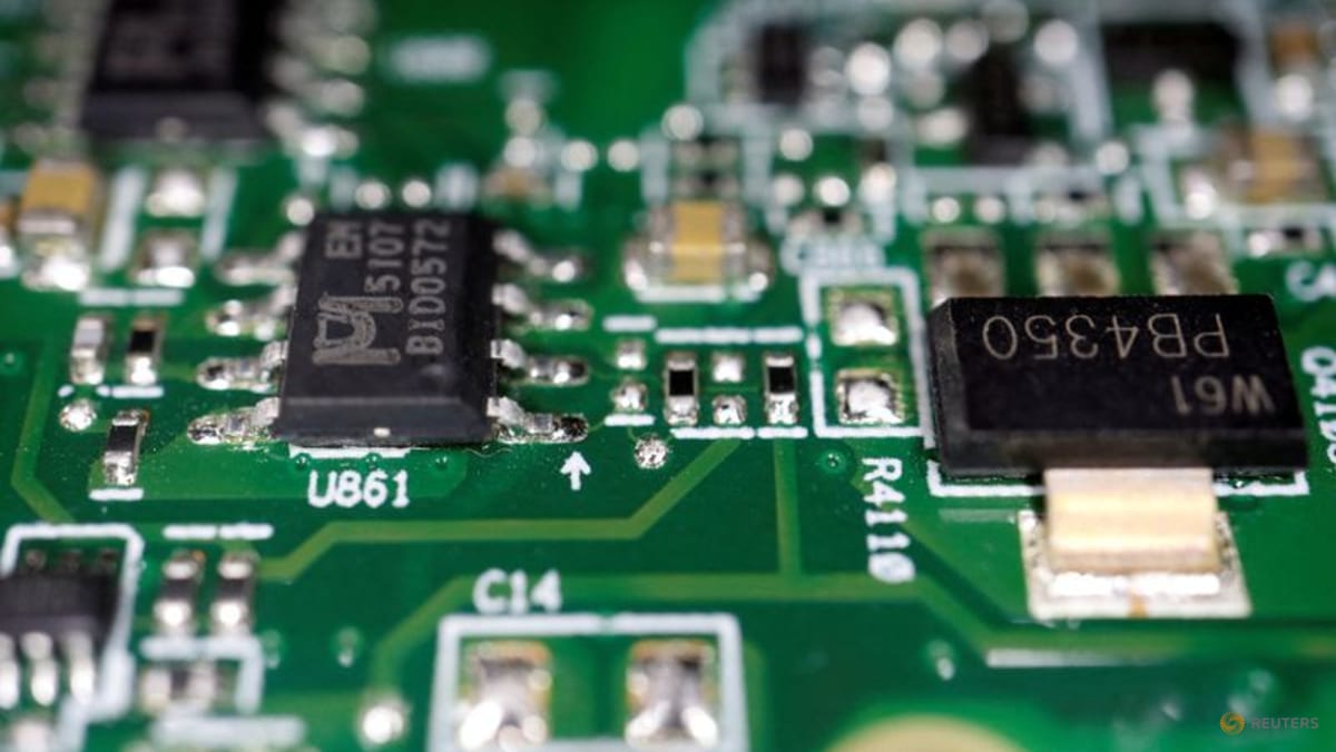
File photo: Semiconductor chips are seen on a printed circuit board in this illustration, taken Feb 17, 2023. (Photo: Reuters/Florence Lo/Illustration)
This audio is generated by an AI tool.
SINGAPORE: Semiconductor industry players have committed more than S$500 million (US$390 million) to research and development projects in Singapore over five years from 2026.
It comes as the country looks to sharpen its edge in advanced chip technologies and help local firms compete in a capital-intensive industry.
Professor Yeo Yee Chia, A*STAR’s deputy chief executive for innovation and enterprise, said Singapore has “one of the most well organised and coordinated ecosystems” globally.
CNA Games Guess Word Crack the word, one row at a time Buzzword Create words using the given letters Mini Sudoku Tiny puzzle, mighty brain teaser Mini Crossword Small grid, big challenge Word Search Spot as many words as you can Show More Show Less “That's what we think is going to make a difference when companies select a location where they can grow their R&D and their business,” he added. THE NEXT FRONTIER IN CHIPMAKING Singapore already accounts for about one in every 10 chips made globally, following years of investment in semiconductor manufacturing and R&D. But the rise of artificial intelligence is placing new demands on chipmakers, just as the conventional route to making computers faster is becoming more difficult.
“That's what we think is going to make a difference when companies select a location where they can grow their R&D and their business,” he added.
THE NEXT FRONTIER IN CHIPMAKING
Singapore already accounts for about one in every 10 chips made globally, following years of investment in semiconductor manufacturing and R&D.
But the rise of artificial intelligence is placing new demands on chipmakers, just as the conventional route to making computers faster is becoming more difficult.
For decades, the industry improved computing performance by packing ever more transistors onto a chip, broadly following a trend known as Moore’s Law.
When the trend was first observed in the 1960s, transistors were measured in micrometres.
Today, some chip features are just dozens of atoms thick, reaching scales where quantum effects become more significant. Pushing the limits further has become increasingly technically challenging and expensive.
Singapore has spent more than a decade developing technologies that could provide alternative ways to improve computing performance.
“I think the next battle will be fought on advanced packaging, heterogeneous integration, chiplets,” said Mr Ravi Krishnaswamy, managing director for Asia-Pacific at growth consulting and market intelligence firm Frost & Sullivan.
“These are areas where I think more economic value-add opportunities will emerge.”
Such technologies would allow more components to be packed closely together, shortening the distance data has to travel and potentially reducing energy use.
Other areas of research include photonics, which uses light rather than electrical signals to move data more efficiently for data-hungry AI systems, as well as chips designed to handle the enormous power requirements of data centres .
BUILDING AN INTEGRATED ECOSYSTEM
A*STAR is also seeing “an increasing pipeline” of overseas companies without a presence in Singapore coming here to work with existing partners, Prof Yeo said.
Mr Krishnaswamy said Singapore’s advantage may lie in its ability to combine different capabilities.
“So it doesn't need to be one niche. I think we can probably bring a lot of these things to the table as an integrated ecosystem capability,” he added.
Infrastructure is another part of the equation.
A*STAR is looking to invest in next-generation tools that firms can tap to gain a competitive advantage.
“By providing our infrastructure, by providing our talent and technology development capabilities, we want to accelerate the companies’ capabilities to go from research to development to manufacturing at speed and at scale,” Prof Yeo said.
LOWERING THE BARRIERS TO INNOVATION
In an industry where global giants spend billions on facilities and talent, small- and medium-size enterprises (SMEs) in Singapore’s semiconductor sector need every edge they can get.
“We want to allow such companies to have an unfair advantage,” Prof Yeo said. “By allowing them to leverage our investment, it lowers the barrier to their R&D and to their ability to innovate and provide solutions.”
Singapore metalens firm MetaOptics is one company that has tapped that support for talent, intellectual property and R&D efforts.
Its CEO Aloysius Chua said raising money remains difficult for young technology companies, regardless of where they are based.
“I think our early supporters are some of the SMEs in Singapore, and then also we have strong support from A*STAR,” he said.
MetaOptics, which has since gone public and taken its products overseas, develops technology for producing flat optical components that can be used in applications ranging from cameras and sensors to high-speed computing connections.
Semiconductor equipment manufacturer NexGen Wafer Systems has similarly benefited from access to shared infrastructure.
Its CEO Cheung Ting Kwan said building all the facilities the company requires itself would mean investing in its own clean room and other specialised equipment.
“If we do it ourselves, this becomes quite prohibitive, expensive for a small- and medium-sized company like us,” he said.
FROM TECHNOLOGY TO CUSTOMERS
But access to infrastructure and talent solves only part of the problem.
For Singapore semiconductor companies, another obstacle is finding enough customers to turn specialised technologies into sustainable businesses.
Advanced Micro Foundry (AMF), a Singapore company working in silicon photonics, was acquired by multinational chipmaker GlobalFoundries last year.
Finding customers for niche technologies was a challenge, said AMF co-founder Patrick Lo.
"We like to build the fab infrastructure, but want it to be fully utilised,” said Mr Lo, who is now a senior fellow of technology development and advanced photonics at GlobalFoundries.
“That full utilisation will be absolutely coming from the application side. This is something I like Singapore as a whole, actually, to have more designers come up, more product developers to leverage.”
It is a challenge some companies are also grappling with as they try to translate breakthroughs into commercial products.
“Maybe people get a lot of funding, but what's after?” Mr Chua said. “If I develop the technology to what it is, and I cannot commercialise it, then I think as a company we've failed.”
Get our pick of top stories and thought-provoking articles in your inbox
Stay updated with notifications for breaking news and our best stories
Join our channel for the top reads for the day on your preferred chat app
据新加坡科技研究局(A*STAR)统计,这超过了2020年至2025年间用于此类工作的4亿多新元。
资料照片:图中所示为印刷电路板上的半导体芯片,拍摄于2023年2月17日。(图片:路透社/Florence Lo/插图)
这段音频由人工智能工具生成。
新加坡:半导体行业参与者已承诺在2026年起的五年内,向新加坡的研发项目投入超过5亿新元(3.9亿美元)。
该国正寻求提升其在先进芯片技术领域的优势,并帮助本土企业在资本密集型行业中展开竞争。
新加坡科技研究局(A*STAR)创新与企业副首席执行官杨怡琪教授表示,新加坡拥有全球“组织最完善、协调性最强的生态系统之一”。
CNA游戏 猜词游戏 逐行破解单词 流行词游戏 用给定的字母组成单词 迷你数独 小谜题,脑力挑战 迷你填字游戏 小方格,大挑战 单词搜索 尽可能多地找出单词 显示更多 显示更少 “我们认为,当企业选择一个能够发展研发和业务的地点时,这一点将会产生影响,”他补充道。 芯片制造的下一个前沿领域 经过多年对半导体制造和研发的投资,新加坡目前在全球芯片产量中约占十分之一。但人工智能的兴起对芯片制造商提出了新的要求,与此同时,传统的提升计算机速度的方法也变得越来越困难。
他补充说:“我们认为,当企业选择一个能够发展研发和业务的地点时,这一点将会产生影响。”
芯片制造的下一个前沿领域
经过多年对半导体制造和研发的投资,新加坡目前在全球芯片产量中约占十分之一。
但人工智能的兴起对芯片制造商提出了新的要求,与此同时,提高计算机速度的传统方法也变得越来越困难。
几十年来,计算机行业通过在芯片上集成越来越多的晶体管来提高计算性能,这大致遵循着被称为摩尔定律的趋势。
20 世纪 60 年代首次观察到这种趋势时,晶体管的尺寸是以微米为单位来衡量的。
如今,某些芯片结构仅有几十个原子厚,达到了量子效应显著的尺度。进一步突破这一极限,在技术上变得越来越具有挑战性,成本也越来越高。
新加坡十多年来一直在开发能够提供提高计算性能的替代方法的技术。
“我认为下一场战斗将在先进封装、异构集成和芯片组领域展开,”增长咨询和市场情报公司弗若斯特沙利文亚太区董事总经理拉维·克里希纳斯瓦米先生表示。
我认为这些领域将会出现更多创造经济价值的机会。
这些技术可以让更多组件紧密地封装在一起,缩短数据传输距离,并有可能降低能源消耗。
其他研究领域包括光子学,它使用光而不是电信号来更有效地传输数据,以满足数据密集型人工智能系统的需求;以及旨在处理数据中心巨大电力需求的芯片。
构建一体化生态系统
杨教授表示,A*STAR 还发现,越来越多在新加坡没有分支机构的海外公司来到这里与现有合作伙伴开展合作。
克里希纳斯瓦米先生表示,新加坡的优势可能在于其能够将不同的能力结合起来。
“所以它不必局限于某个特定领域。我认为我们可以将很多这类东西整合到一个综合的生态系统能力中,”他补充道。
基础设施是另一个重要因素。
新加坡科技研究局 (A*STAR) 正在寻求投资下一代工具,以便企业能够利用这些工具获得竞争优势。
“通过提供我们的基础设施、人才和技术开发能力,我们希望加快企业从研发到生产制造的进程,实现速度和规模上的飞跃,”杨教授说。
降低创新门槛
在全球巨头斥资数十亿美元用于设施和人才的行业中,新加坡半导体行业的中小企业需要尽可能地争取优势。
“我们希望让这些公司拥有不公平的优势,”杨教授说。“通过允许他们利用我们的投资,可以降低他们研发的门槛,增强他们创新和提供解决方案的能力。”
新加坡超透镜公司 MetaOptics 就是一家利用这种支持来发展人才、知识产权和研发工作的公司。
其首席执行官 Aloysius Chua 表示,无论总部设在哪里,年轻的科技公司筹集资金仍然很困难。
“我认为我们早期的支持者是新加坡的一些中小企业,此外,我们也得到了新加坡科技研究局(A*STAR)的大力支持,”他说。
MetaOptics 公司已上市并将其产品推向海外,该公司开发用于生产平面光学元件的技术,这些元件可用于从相机和传感器到高速计算连接等各种应用。
半导体设备制造商 NexGen Wafer Systems 也同样受益于共享基础设施。
其首席执行官张廷坤表示,自行建造公司所需的所有设施意味着要投资建设自己的洁净室和其他专用设备。
他说:“如果我们自己做,对于像我们这样的中小型企业来说,成本会非常高昂,难以承受。”
从技术到客户
但是,获得基础设施和人才只能解决部分问题。
对于新加坡半导体公司而言,另一个障碍是找到足够的客户,将专业技术转化为可持续发展的业务。
去年,从事硅光子学研究的新加坡公司 Advanced Micro Foundry (AMF) 被跨国芯片制造商 GlobalFoundries 收购。
AMF联合创始人Patrick Lo表示,为小众技术寻找客户是一项挑战。
“我们喜欢建设晶圆厂基础设施,但希望它能得到充分利用,”罗先生说道,他现在是 GlobalFoundries 技术开发和先进光子学的高级研究员。
“这种资源的充分利用绝对要归功于应用方面。实际上,我个人很希望新加坡能涌现出更多设计师和产品开发人员,以便更好地利用他们的才能。”
这也是一些公司在努力将突破性成果转化为商业产品时所面临的挑战。
“或许有人能获得大量资金,但之后呢?”蔡先生说,“如果我把技术开发到现在的水平,却无法将其商业化,那么我认为我们公司就失败了。”
订阅我们的邮件,即可获取精选热点新闻和引人深思的文章。
订阅通知,第一时间获取突发新闻和精彩报道。
加入我们的频道,即可在您常用的聊天应用上获取当日热门文章。